As a technological pioneer in China's power semiconductor sector, Alkaidsemi has completed the iteration of five generations of SiC MOSFET products. The team has accumulated over 20 years of experience in this field and taken the lead in establishing a fully domestic supply chain system to ensure the safety and stability of the supply chain.
With the mass production and application of the company's fifth-generation SiC MOSFETs, Alkaidsemi is helping users address the core pain points in SiC applications and driving the third-generation semiconductor technology to create value in more fields.
Technological Innovation Simplifies Drive Design and Enhances System Reliability
In high-efficiency application fields such as new energy vehicles, AI server power supplies, photovoltaic energy storage, and charging piles, SiC MOSFETs are rapidly replacing traditional silicon-based devices due to their excellent switching performance and high-temperature conduction advantages. However, in practical applications, they face a tricky problem - traditional planar-structured SiC MOSFETs must adopt negative-voltage turn-off.
This limitation not only increases system complexity and cost but also becomes an invisible barrier to the popularization of SiC technology. Now, through technological innovation, Alkaidsemi has successfully launched the fifth-generation planar-structured SiC MOSFETs that support zero-voltage turn-off, bringing a brand-new solution to the industry.
Reasons for Negative-Voltage Turn-Off Requirement of Traditional Planar SiC MOSFETs
SiC MOSFETs have faster switching speeds and higher dv/dt characteristics than silicon-based devices. But this advantage may affect application effects in practical bridge circuit applications.
In the power electronics field, the bridge circuit is one of the most common topological structures. As shown in Figure 1, when the lower MOSFET turns off, the midpoint potential of the bridge arm rises sharply. The generated high-speed dv/dt will produce a positive crosstalk voltage ΔVgs at the gate of the lower MOSFET through the Miller capacitance (Cgd) of the lower MOSFET and the drive resistor Rg. Once this crosstalk voltage exceeds the device threshold voltage Vgs(th), it will cause the lower MOSFET to conduct again, resulting in a direct short circuit of the bridge arm and instant damage to the device. Similarly, the turn-on and turn-off of the upper MOSFET will cause positive and negative crosstalk at the gate of the upper MOSFET respectively.
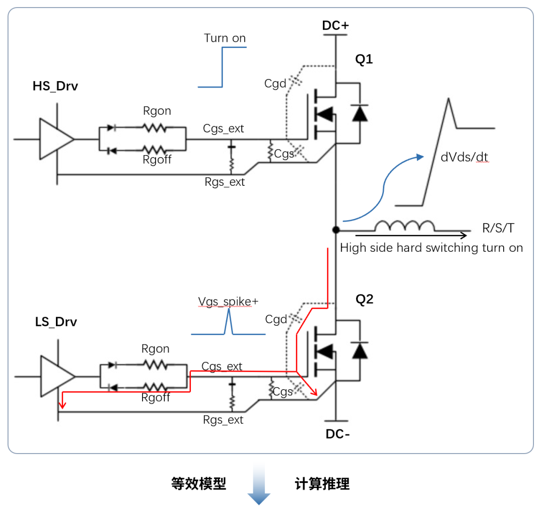
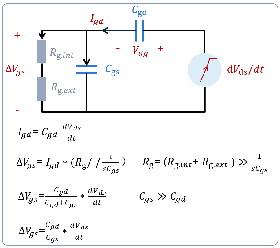
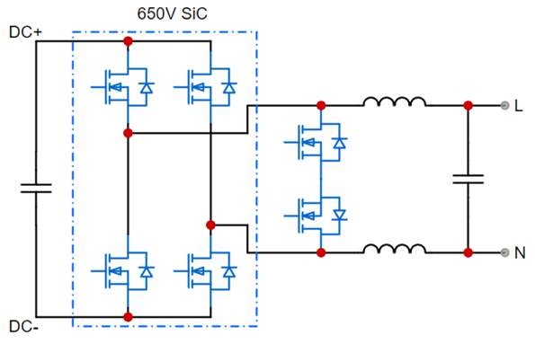
Figure 1
The threshold voltage for turning on SiC MOSFETs has a negative temperature coefficient characteristic - as the temperature rises, Vgs(th) decreases. This means that under high-temperature operating conditions, the anti-interference ability of the device weakens and the risk of false conduction increases.
The traditional solution adopts a negative-voltage turn-off method of -3V to -5V. A negative voltage is applied to the gate to ensure that the gate-source voltage (Vgs) is far lower than the threshold voltage and establish a safety buffer zone.
Although this solution is effective, it brings significant side effects:
-
Increased cost: Additional negative-voltage power supply circuits (zener diodes, charge pumps, etc.) are required.
-
Complex design: The complexity of the drive circuit doubles, and Layout challenges increase.
-
Reliability risks: The negative-voltage circuit itself may become a new fault point.
The complex negative-voltage drive solution and the risk of device damage have seriously restricted the promotion of SiC MOSFETs in high-efficiency systems.
Alkaidsemi's New Breakthrough: Zero-Voltage Turn-Off Technology
To address this pain point, Alkaidsemi has achieved a revolutionary breakthrough in its fifth-generation 650V planar-structured SiC MOSFET products. After repeated verification in laboratories and by clients, 0V turn-off is completely feasible and reliable, providing a better choice for the market.
This innovation is not accidental but stems from Alkaidsemi's profound understanding of the core mechanism and application of devices. In December 2023, the "Key Technology for High-Reliability SiC Devices" project developed by Alkaidsemi received high recognition from an evaluation committee led by domestic academic circles and was rated at the "internationally advanced" level.
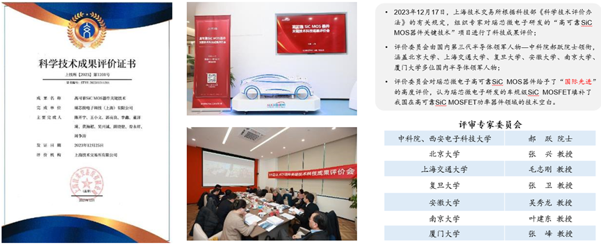
Figure 2
Verification by Measured Data
Verification method: Based on a typical double-pulse test circuit (as shown in Figure 3), fix the working state of the drive tube, adjust the turn-off voltage of the freewheeling tube, and accurately capture the reverse recovery current waveform of the freewheeling tube at the moment the drive tube is turned on. Then extract the reverse recovery charge Qrr. If the total Qrr increases significantly, it indicates obvious crosstalk effects. Therefore, the variation of Qrr directly reflects the anti-crosstalk ability of the device.
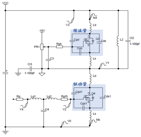
Figure 3 Schematic Diagram of Typical Double-Pulse Test
Test conditions:
Drive tube VGS = -4V/18V, freewheeling tube turn-off voltage varies from -4V to +2V
Gate resistance Rgon = 10Ω, Rgoff = 3.3Ω
Drain current Ids = 30A
Test results and analysis:
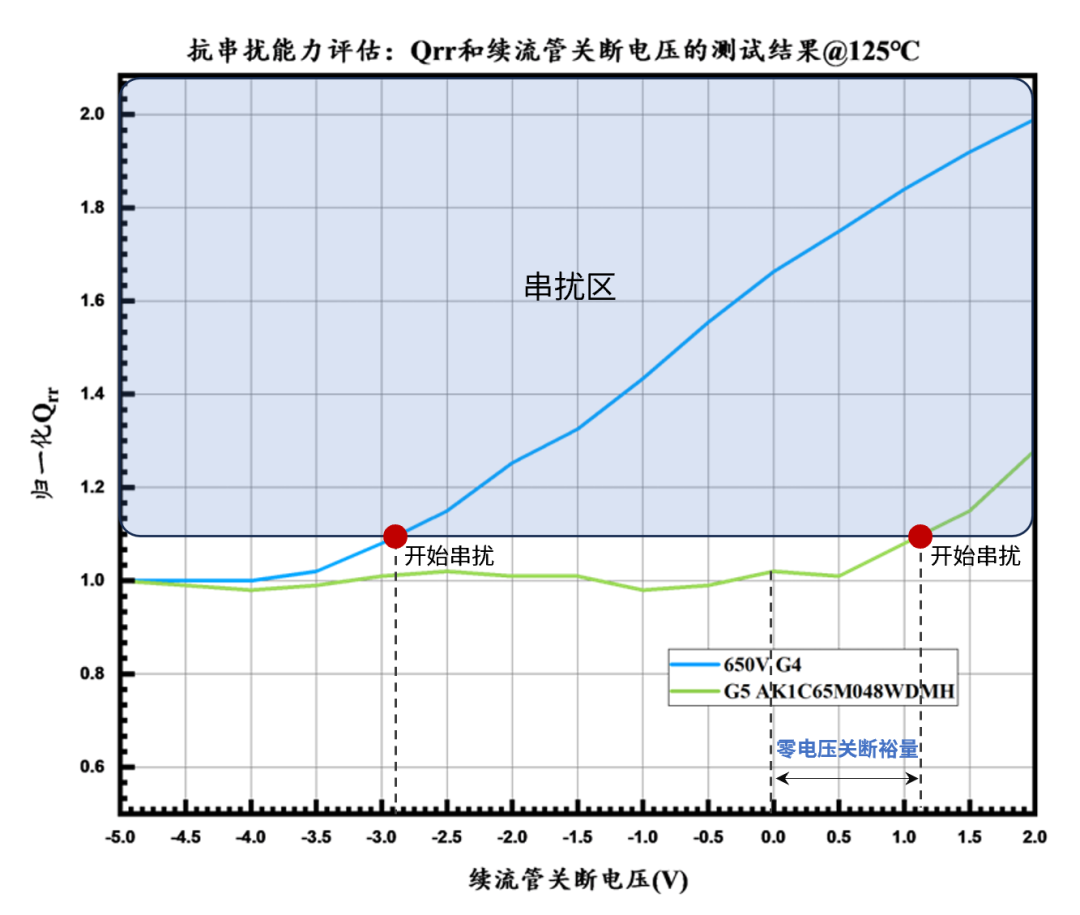
Figure 4 Relationship Between Anti-Crosstalk and Turn-Off Voltage
The test results show that Alkaidsemi's product AK1C65M048WAMH has minimal Qrr variation under the conditions of fast (Rgoff = 3.3Ω) turn-off and turn-off voltage less than 2V, and the crosstalk effect is almost negligible. This means that the product can meet zero-voltage turn-off at a high temperature of 125℃ with a margin of more than 1V. This benefit comes from Alkaidsemi's continuous innovation in device structure design, gate drive optimization, and packaging technology, ensuring the high reliability and stability of the device in high-frequency, high-voltage, and high-temperature environments.
Multiple Values Brought by Zero-Voltage Turn-Off
The zero-voltage turn-off characteristic of Alkaidsemi's fifth-generation SiC MOSFETs brings multiple revolutionary advantages to power electronics design:
1
Significant simplification of drive circuits
No negative-voltage power supply circuit is needed, and only a single positive power supply drive (such as 0V turn-off / 18V turn-on) is required. This not only reduces the number of components but also simplifies PCB layout design and lowers the design difficulty for engineers.
2
Remarkable reduction in system cost
It eliminates the need for components required for negative-voltage generation (special drive ICs, zener diodes, additional capacitors, etc.), reducing BOM costs. This is particularly important for cost-sensitive applications.
3
Overall improvement in reliability
It eliminates potential fault points that may be caused by the negative-voltage circuit itself, improving the overall reliability of the system. At the same time, the optimized device performs more stably and reliably in high-temperature environments.
4
Shortened design cycle
There is no need to spend a lot of debugging time on negative-voltage design, isolation, and potential crosstalk issues, accelerating the product launch process.
Empowering High-Efficiency Application Scenarios
Alkaidsemi's fifth-generation SiC MOSFETs have demonstrated excellent performance in several key fields:
On-Board OBC and AI Server Power Supplies
In the totem-pole PFC fast bridge arm, combined with the zero-voltage turn-off characteristic, the server power supply efficiency can easily exceed the titanium standard. At the same time, the drive circuit area is reduced by about 10%, helping to improve power density.
Residential Inverters
In the Heric inversion of residential photovoltaic systems, the 650V SiC MOSFET platform supporting 0V turn-off significantly improves system efficiency and power density through optimizing device performance, simplifying topological design, and hybrid application with silicon-based devices. It also reduces common-mode noise.