As the new energy vehicle market enters a deep development phase, the on-board charger (OBC) is undergoing a disruptive transformation from a "functional component" to a "smart energy node". Trends such as high power density, low energy consumption, compatibility with 800V platforms, and V2L/V2G bidirectional interaction have posed unprecedented challenges to power devices. Leveraging its in-depth layout in the power semiconductor field, Alkaidsemi has taken the lead in launching a full-stack power device solution, redefining the benchmarks for OBC power density and energy efficiency.
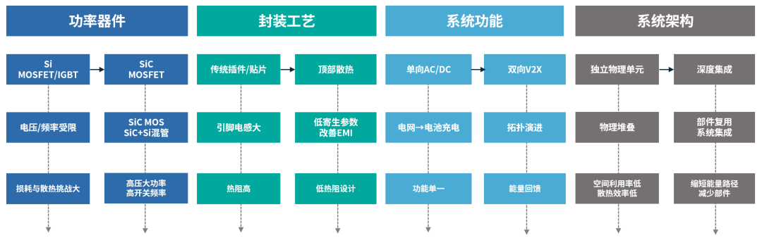
Figure 1. Key Technological Evolution and Trends of OBC
The key technological evolution of OBC can be summarized across four core dimensions
Power Device Technology Enters the Wide Bandgap Era
With the rapid transition of automotive battery voltages to 800V and the mass adoption of wide bandgap devices such as SiC MOSFETs, OBC performance has achieved generational leaps. These devices deliver far superior performance to silicon-based devices in high-frequency, high-voltage, and high-temperature scenarios, enabling system efficiency to easily exceed 96% and helping the overall power density reach or even surpass the 4kW/L milestone. High-performance devices have become the core driving force behind the high power density, lightweight, and compact design of OBCs.
Packaging Technology Advances Toward High Power Density and Low Thermal Resistance
In terms of packaging forms, OBC power devices are undergoing significant structural upgrades:
Through-Hole: Common in early solutions, offering stable installation but suffering from high losses, large volume, and disadvantages for EMI and high-density integration.
SMD: Enables more compact layouts and lower parasitic parameters, emerging as the current mainstream.
Top-side cooling: Aligned with the trends of 800V and high-power OBCs, it significantly reduces thermal resistance and improves thermal cycle life, allowing modules to carry higher power in an ultra-small form factor and becoming a key focus for future high-end platforms.
Packaging evolution and device performance upgrades complement each other, jointly supporting the OBC system to move toward higher power density and efficiency.
Functions Expand from Unidirectional Charging to Bidirectional Energy Nodes
The OBC is no longer merely a device that "charges AC power into the battery", but is gradually evolving into a bidirectional energy port for vehicles. Its functions have expanded from unidirectional charging to multi-scenario applications such as V2G (Vehicle-to-Grid), V2L (Vehicle-to-Load), and V2H (Vehicle-to-Home). In the future, it will also be deeply integrated into the vehicle's domain control system, enabling the intelligent integration of vehicle energy scheduling, thermal management, and load management.
System Architecture Continues to Evolve Toward Higher Integration
OBC solutions are transitioning from the early "two-stage structure (AC/DC + DC/DC)" to more efficient "single-stage topologies", and further moving toward "deep integration" (where OBC and low-power DC-DC share transformers, power bridges, and MCUs). Integrated design can effectively shorten wiring harness lengths, reduce the number of components, achieve a 30%-50% reduction in volume and a 20% reduction in weight, while improving system conversion efficiency and operational reliability.
Alkaidsemi's Advantages: Complete Device Matrix + Comprehensive Performance Leadership
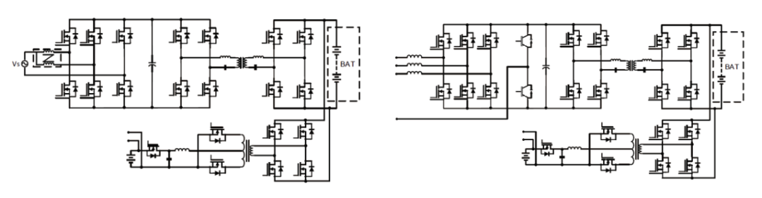
Figure 2. Common Topology System for OBC + DC/DC
From the front-end PFC of OBC, to the core CLLC/DAB isolated conversion, and further to the mid-to-back-end SR and ORing in HV-LV DC/DC, Alkaidsemi offers IGBT + Si FRD discrete devices, IGBT + JBS hybrid devices, SiC MOS, and SGT MOS, providing customers with a true full-stack power device platform.
Zero Defect Engineering: Rigorous Quality Control
Against the backdrop of extremely high safety and reliability requirements for on-board OBCs, Alkaidsemi has built a comprehensive zero-defect management process (Zero Defect AEC-Q004) based on a stringent automotive-grade quality system. From the design source to the mass production closed loop, every link adheres to a systematic quality control logic:
-
Product Design Phase: Conduct multi-dimensional verification of structure, electrical performance, and thermal characteristics based on simulation and modeling. Guided by robust design principles, strictly implement DFMEA to ensure potential failures are systematically identified and mitigated before mass production.
-
Manufacturing Phase: Wafer fabrication and packaging factories comply with ISO9001/IATF16949 quality system requirements and possess VDA6.3 customer audit capabilities. Process stability and consistency are ensured through process audits and safe mass production mechanisms.
-
Testing Phase: Full-process coverage of CP, FT and other test items, based on automotive-grade statistical process control (SPC) standards, to ensure shipment consistency and failure traceability.
-
Environmental and Stress Verification: Products must pass enhanced tests such as Extended Reliability and ORT (Ongoing Reliability Test), covering multiple scenarios including temperature, humidity, and electrical stress, to ensure long-term reliability in complex vehicle systems.
-
Continuous Improvement Mechanism: Establish a real-time defect monitoring system for wafer fabrication and packaging/testing processes, and implement change control for all key processes to ensure the robustness of products throughout their life cycle.
-
Rapid Problem-Solving Capability: Adopt systematic problem analysis and failure mechanism analysis methods, and establish a rapid response mechanism to ensure the closed-loop resolution of on-site customer issues.
Relying on the above six quality system capabilities, all of Alkaidsemi's automotive-grade products meet the requirements of AEC-Q100/Q101/Q104/Q006 standards and provide complete PPAP support, achieving true "automotive-grade reliability" assurance and serving as a reliable chip foundation for core new energy vehicle systems including OBCs.
Deep Collaboration with Customers from Device to System
Through its full-stack power device layout, Alkaidsemi provides customers with a complete OBC platform-level solution from front-end AC-DC to back-end HV-LV DC-DC, offering a "Solution Selling" support system that includes:
-
Recommendations for OBC/DC-DC device matching solutions (Si/SiC/SJ/IGBT) and application guidance
-
Accurate Spice Models and sixth-order thermal resistance models
-
Full-link application reference designs
-
Expertise in EMI suppression and switching noise reduction
-
On-site technical support
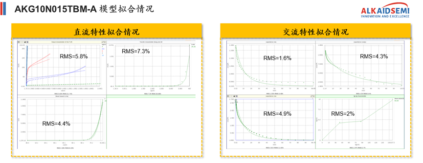
Figure 3. Spice Model Fitting of AKG10N015TBM-A
Success Case
A 6.6kW bidirectional SiC solution co-developed with a leading OBC manufacturer completed the process from device selection to DV verification in just six months, achieving a power density of 105W/in³ and an efficiency of >97%, setting a new benchmark for high-end vehicle models in 2025.
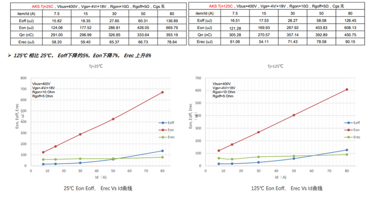
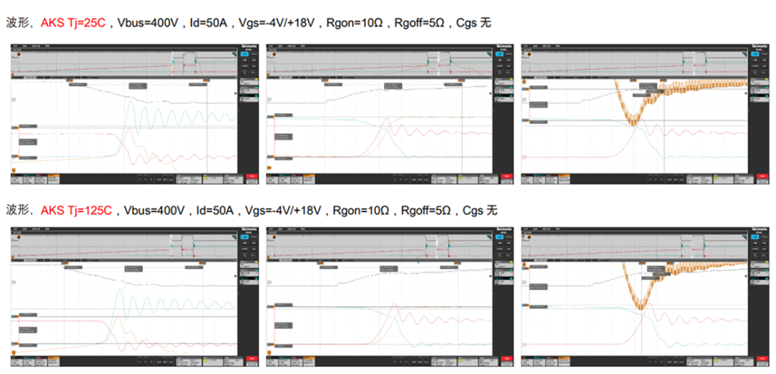
Figure 4. Providing Customers with Device Parameter Testing
Defining the Next Decade of OBC
The technological revolution of OBC is far from over—optimizations for higher efficiency, greater compactness, and enhanced reliability are underway. Our mission is to make high-end technology accessible to the entire new energy vehicle industry.
For OBC power device selection or solution optimization needs, we welcome your inquiries at any time!