1. Introduction to the New Platform
1.1 Platform features
Alkaidsemi (Shanghai) Electronic Technology Co., Ltd. has leveraged its advanced technology to launch the 1200V G4.5 technology platform AK1CK2MXXX series SiC MOSFETs, achieving significant improvements in both on-resistance and dynamic performance. These superior performance advantages not only enhance energy conversion efficiency but also reduce system power consumption, delivering a more efficient and reliable user experience. Whether in the electric vehicle sector or other new energy applications, the AKS 1200V G4.5 technology platform demonstrates strong competitiveness. Take the 1200V G4.5 40mΩ (AK1CK2M040WAM) as an example, which is primarily used in OBC (on-board chargers) – an application with extremely high requirements for parasitic capacitance CGD. This product features a CGD parameter of less than 10 pF, resulting in substantial reductions in switching losses. Concurrently, the next-generation G5 products scheduled for launch next year will achieve outstanding technological upgrades, further reducing RON,SP (specific on-resistance).
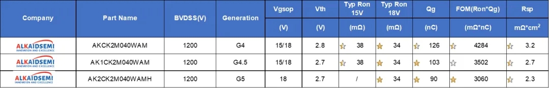
Figure 1 Comparison of AKS 1200V SiC MOSFETs Technology
1.2 Product Distribution

Table 1 AKS 1200V G4.5 SiC MOSFETs series products
The 1200V G4.5 technology platform has multiple specifications and packaging forms ranging from 14-80m Ω to match different topology circuit applications.
2. Technical Parameter
2.1 Device Quality
Power devices typically use RON, SP (specific on resistance), and FOM (quality factor) to measure device performance.
The RON and SP of the 1200V G4.5 platform product have decreased by 16% compared to the previous generation G4 platform product. In the future, it is expected that the RON and SP will decrease by another 12% and FOM will decrease by another 10% on the G5 platform.

Figure 2 Normalized RON of AKS SiC MOSFETs, SP:G4 vs. G4.5 vs. G5
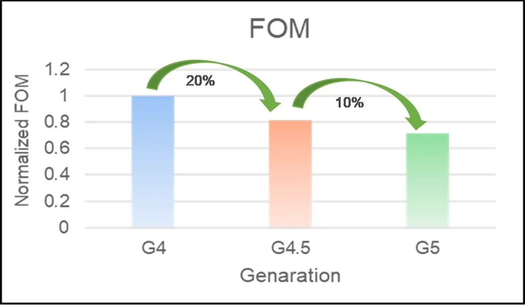
Figure 3 Normalized FOM of AKS SiC MOSFETs: G4 vs. G4.5 vs. G5
2.2 Temperature Rise
In practical applications, the on resistance of power devices is not constant. The typical value of on resistance in the specification book usually refers to the on resistance of the device at room temperature. In high-power applications, the device usually operates at higher junction temperatures. Therefore, it is necessary to know the on resistance performance of the device at high temperatures.
The on resistance of the 1200V G4.5 platform product is lower than that of the G4 platform product of the same specification under various temperature conditions. At room temperature, the on resistance decreases by 9%, and at a high temperature of 175 ℃, the resistance decreases by 3%. The decrease in on resistance value means that the static power consumption of the device will be smaller, and the range of power applications available will be wider.
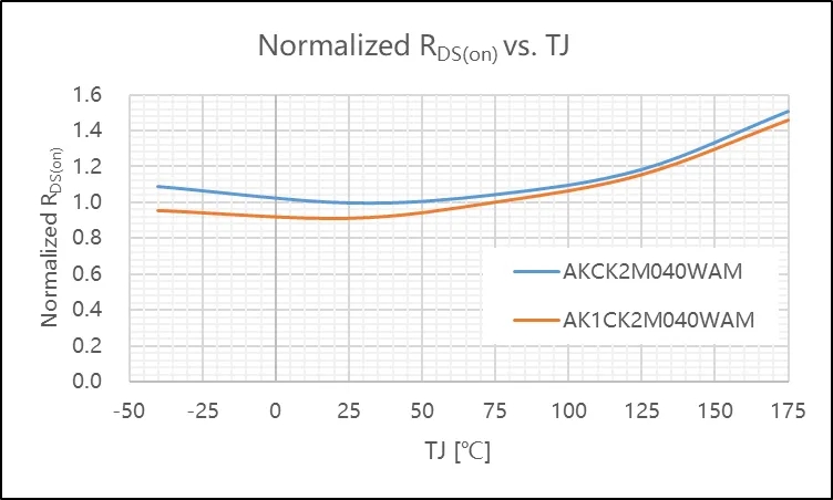
Figure 4 Normalized RDS (ON) of AKS SiC MOSFETs at different junction temperatures: G4 vs. G4.5
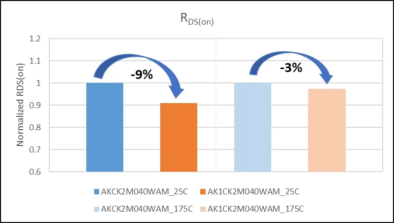
Figure 5 AKS SiC MOSFETs normalized RDS (ON) at room temperature and high temperature: G4 vs. G4.5
2.3 Charge
The gate charge QG represents the amount of charge required to drive the gate of a device. In some fast switching applications, a smaller gate charge indicates faster device turn-on and turn off speeds, which can reduce dynamic losses of the device.
The QG of 1200V G4.5 platform products decreased by 20%, and the parasitic conductivity factor (PTO) decreased by 44% (PTO)= QGD@800V / QGS@VTH_25C )By increasing the switching speed, the possibility of parasitic conduction is reduced.
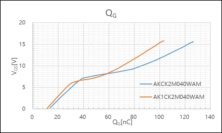
Figure 6 AKS SiC MOSFETs QG: G4 vs. G4.5

Figure 7 AKS SiC MOSFETs PTO: G4 vs. G4.5
2.4 Output Capacitance
The output capacitance COSS is one of the important indicators that determine the switching loss of devices, and the dynamic loss EOSS generated by it plays an important role in the switching process, which will affect the efficiency of the system in topology circuit applications.
Compared to G4 platform products, 1200V G4.5 platform products have lower output capacitance, optimized product EOSS/QOSS, and can effectively reduce dynamic losses in applications.

Figure 8 AKS SiC MOSFETs COSS: G4 vs. G4.5
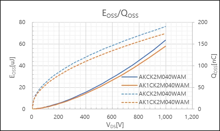
Figure 9 AKS SiC MOSFETs Eoss/QOSS: G4 vs. G4.5
2.5 Double Pulse Test
Double pulse testing is a commonly used testing method to characterize the dynamic characteristics of devices. Through device design optimization, the switching losses of the 1200V G4.5 platform product in double pulse testing are better than those of the G4 platform product, and the reverse recovery charge of its body diode is also reduced by 6%.

Figure 10 AKS SiC MOSFETs with different RG (EXT) switching losses: G4 vs. G4.5

Figure 11 AKS SiC MOSFETs Qrr: G4 vs. G4.5
2.6 Efficiency Testing
In a 30kW air-cooled 2U charging pile, the three-phase LLC section is tested using 1200V 40m Ω silicon carbide MOS efficiency comparison. Under 60-100% load, the G4.5 platform shows a 0.01-0.04% increase in efficiency compared to the G4 platform's equivalent Rdson product.
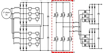
Figure 12 SiC application in three-phase LLC expansion and compensation
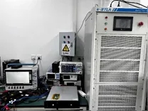
Figure 13 30kW air-cooled 2U charging station module

Figure 14 Conversion efficiency of AKS SiC MOSFETs under different loads: G4 vs. G4.5