Technical Sharing | Analysis of Voltage Stress during Gate Miller Platform Vibration
Release time: 2025-01-05

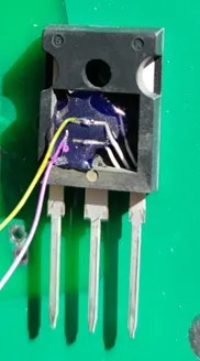
During the switching process of the MOS, the gate voltage is prone to oscillation, generating very high or very low voltage spikes. The externally measured Vgs value may far exceed the maximum value allowed in the device specification sheet. Users often worry that excessive gate stress may lead to damage to the device's gate.


This phenomenon occurs in devices without Kelvin pins (such as TO247 - 3), mainly due to the parasitic inductance L of the source (including the soldered pins and bonding wires). According to the formula U = L * di/dt, a high switching speed, that is, a large di/dt, results in a greater induced voltage on the parasitic inductance of the source pin. At this time, the externally measured voltage Vgs is mainly the internal Cgs voltage superimposed with the induced voltage on the S parasitic inductance (3 - 7 nH).
Generally, during fast turn - off (which varies with different drivers and currents), the di/dt is approximately 5000 - 20000 A/μs, that is, 5 - 20 A/ns. At this time, the induced voltage on the S pin (3 nH) is about 15 - 60 V.

Since the MOS is still in the Miller plateau stage at this time, the Miller plateau voltage of Vgs is approximately 5 - 7 V. Therefore, the externally measured voltage Vgs (external) is the sum of the Miller plateau voltage and the induced voltage on the S pin, resulting in a very high spike.

To test the difference between the internal and external GS voltages of the MOS, a window is opened on the MOS to expose the bonding wires. Then, wires are soldered from the bonding wires near the chip to measure the GS voltage (the measured waveform here represents the real GS waveform of the MOS). At the same time, a differential probe is placed close to the GS pins of the MOS to represent the conventional testing method (the externally measured waveform of the MOS). An experiment is conducted to compare the internal and external Vgs waveforms during switching.

Modification of Window MOS and Testing Reference (1)

Modification of Window MOS and Testing Reference (2)


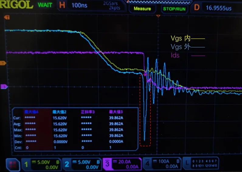
The measured MOS turn off waveform is as follows:

The Vgs voltage measured externally will have a significant negative peak (about 20V) when Ids suddenly drops. At this point, the internal Vgs remains almost unchanged (slight fluctuations are mainly caused by electromagnetic interference during sudden changes in current and voltage).


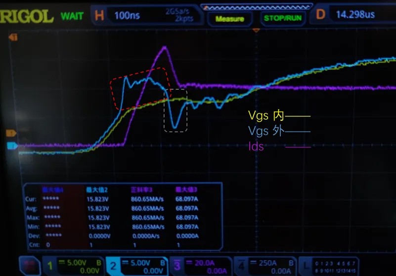
The measured MOS open waveform is as follows:

The externally measured Vgs voltage will have a positive rise when Ids rises, while the reverse recovery edge will cause the external Vgs to synchronously decrease when Ids falls. At this point, the internal Vgs remains almost unchanged (slight fluctuations are mainly caused by electromagnetic interference during sudden changes in current and voltage).


Summary

At the oscillation point of the Miller platform, the large peak voltage measured externally by Vgs is generated by the parasitic inductance of the source pin inducing voltage at high di/dt superimposed on the Miller platform voltage. At this point, the external measurement value does not represent the true voltage of Vgs inside the MOS at all. The external measurement voltage spike is a true reflection of the size of the didt mutation.

At this point, the actual Vds will also undergo a sudden change, and Cgs will be charged through the Cgd capacitor. Therefore, the actual Vgs voltage inside will also change due to the sudden change in Vds voltage. The theoretical limit change value is determined by the Δ Qgd value and Cgs size caused by the change in Δ Vds. For example, if Δ Qgd 10nC and Cgs 10nF, the maximum change in Vgs at this time is 1V. As the MOS operates in the saturation region (Miller plateau), a slight change in internal Vgs (such as a 0.5-1V change) can cause a significant jump in channel saturation current. Due to the fact that the internal true Vgs often cannot be measured, the change in Ids can be used to evaluate the internal true Vgs change in reverse. (Different saturation currents correspond to different Vgs voltages, and there are output curves in the device specification book).

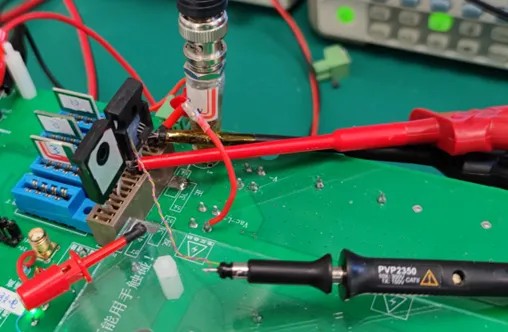
In addition, measuring the external Vgs voltage during the operation of high-voltage devices is also difficult, as common measurements often use differential probes. It is necessary to pay attention to the common mode suppression performance of differential probes at high frequencies (often 100MHz), as poor common mode suppression performance cannot accurately measure the external Vgs voltage. So using an optically isolated probe is an ideal method for measuring external Vgs voltage.


Together for an Intelligent and Sustainable Future

Copyright © 2024 Alkaidsemi (Shanghai) Electronic Technology Co., Ltd.