RLC series resonant circuit
The series RLC circuit consists of a resistor, a capacitor, and an inductor connected in series on an AC power source, as shown in Figure 1.
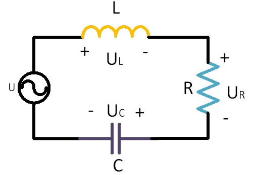
Figure 1: Series RLC Circuit
The calculation formula for the total input impedance of an RLC resonant circuit is Zin=XL+XC+R=wL+1/jwC+R. Finally, it is resolved into the following formula:
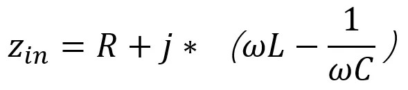
WL is the absolute value of inductive impedance, and 1/wc is the absolute value of capacitive impedance. In the total input impedance, inductive impedance and capacitive impedance can cancel each other out.
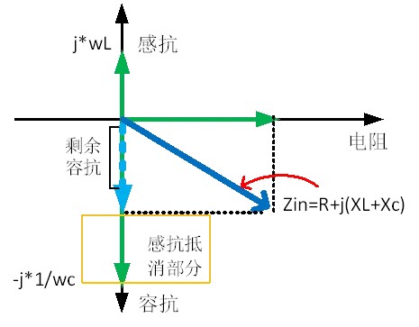
Figure 2 Schematic diagram of capacitive impedance greater than inductive impedance
In Figure 2, after the cancellation of inductive and capacitive reactance, there is still capacitive reactance left. The capacitance and pure resistance vectors are added together. According to the parallelogram rule, the arrow indicates the negative half axis of the final impedance on the Y-axis, so the impedance of the entire circuit is capacitive.
On the contrary, after the cancellation of inductive and capacitive reactance, there is still inductive reactance left, and the impedance of the entire circuit is inductive, as shown in Figure 3.
Figure 3 Schematic diagram of inductive impedance greater than capacitive impedance
When the inductance and capacitance in the series resonant circuit are completely cancelled out, the impedance of the entire circuit becomes resistive, and a frequency f0 can be calculated.
XL=XC,approach
At the frequency point f0, the inductance and capacitance are short circuited relative to the input voltage. Therefore, the voltage at both ends of R is equal to the input voltage Uin.
When the input frequency f is greater than the frequency f0, the inductive reactance will increase and the capacitive reactance will decrease. The entire circuit is inductive and can be equivalent to a series connection of inductors L and R, as shown in Figure 4. The higher the frequency, the greater the inductive reactance, while R remains constant. According to the principle of voltage division, the larger the UL, the smaller the UR.

Figure 4: Equivalent Circuit of f>fo
On the contrary, when the input frequency is less than f0, the capacitive reactance will increase while the inductive reactance will decrease. The entire circuit is capacitive and can be equivalent to a series connection of inductors C and R, as shown in Figure 5. The smaller the frequency, the larger the capacitance impedance, and the higher the capacitance voltage Uc, while the smaller the UR.
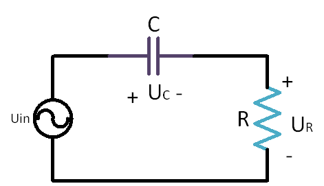
Figure 5 f
Based on the above analysis, it can be concluded that changing the input frequency f can change the resistance voltage UR. At the frequency point f0, the voltage is highest and equal to the input voltage Uin. The trend of UR changing with input frequency is shown in Figure 6.
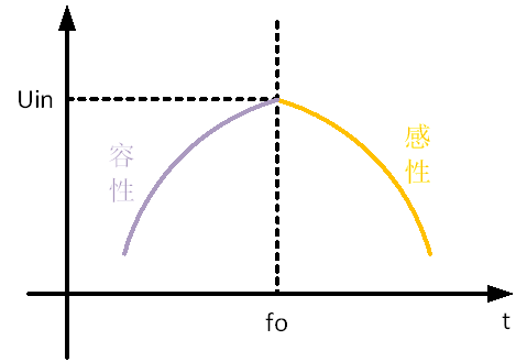
Figure 6 Voltage/Frequency Variation Curve
Quality Factor
Due to the series connection of the entire circuit, when the input frequency f is constant, the UL and Uc voltages are also fixed. As long as the resistance R changes, the UL and Uc voltages will change. As R increases, the loop current Iin decreases, and UL and Uc decrease. In a resonant circuit, the R corresponding to different loads also varies, so the quality factor Q is used to measure the load variation.
The quality factor is the ratio of the power (reactive power) stored on the energy storage device (inductor, capacitor) to the active power consumed by the resistor R. Due to the series connection,
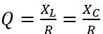
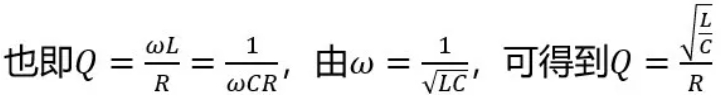
The quality factor Q is a dimensionless number that affects many characteristics of resonant circuits and is an important parameter often used in the study of resonant circuits. It should be emphasized that at the resonant frequency f0, the ratio of inductive impedance to resistance or the ratio of capacitive impedance to resistance is called the quality factor Q.
According to the formula for calculating the quality factor Q in a resonant circuit, when L and C are set, the larger R, the higher the output voltage. If the output voltage is constant, it means that the lighter the load (the larger the R), the smaller the Q.
Therefore, the size of Q represents the weight of the output load, with Q carrying a large load and Q carrying a small load. When drawing LLC curves, different Q values represent different loads.
Gain Relationship
The ratio of output voltage to input voltage is called gain, usually represented by G, G=UR/Uin。 When the frequency is f0, the maximum gain G=1, as shown in Figure 7.
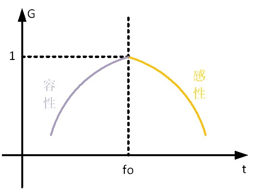
Figure 7 Relationship curve between frequency and gain
In the RLC resonant circuit, when the input frequency f=f0, regardless of the magnitude of R, the gain G is equal to 1. If the input frequency is not at f0, the gain will be different when R is different.
When the frequency f>f0, f is in the inductive region, that is, after the inductive reactance cancels out the capacitive reactance, there is still some inductive reactance left. The entire circuit can be considered as an inductor connected in series with a resistor. At this point, the smaller R, the greater the ratio of inductive impedance XL to resistance R. This way, the smaller the UR. Conversely, the larger the resistance R, the larger the UR.
Therefore, it can be concluded that at the same frequency, the larger the resistance R, the greater the gain.
Conversely, when f is less than f0, the capacitive reactance is greater than the inductive reactance, and the entire circuit is in the capacitive region. When f1 is fixed, the capacitance is fixed, and the larger the resistance, the greater the voltage division, resulting in a larger gain.