Foreword
Three-phase Vienna PFC is a three-level PWM rectifier topology, which aims to improve the efficiency and power factor of power supply system. Because it needs few switching devices, the maximum voltage borne by a single power device is half of the output bus voltage, there is no need to set the driving dead time, and there is no bridge arm straight-through problem, which is widely used. The power semiconductor device of Vienna PFC rectifier is mainly composed of 6 insulated gate transistors (IGBT) and 12 fast recovery diodes (FRD). In this topology application, all IGBT and FRD are hard switches, and the switching loss of power devices is calculated by turning on energy Eon and turning off energy Eoff. The conduction loss of the device is calculated by calculating the conduction current and the saturation (on-state) voltage of the device.
Basic working mechanism of three-phase Vienna PFC
For three-phase three-wire Vienna rectifier, any one of the three phases A, B and C can form a closed loop with the other two phases. Let's take phase A as an example to analyze the commutation path of current.
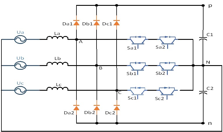
Figure 1 Topology of Three-level Vienna Rectifier
When a phase current is positive:
1 level: When the switch Sa1 is turned off, the output of phase A is positive, that is, UAN=Udc /2, where Udc is the voltage between the positive bus P and the negative bus N.. The current flow path is: flowing from the positive pole of the A-phase power grid, passing through the inductor La, then flowing through the diode Da1 to the DC-side capacitor C1, and finally returning to the A-phase power grid through the other two phases. The specific flow path is shown in Figure 2(a). At this stage, the inductor La and the power grid Ea charge the capacitor and supply power to the post-load.
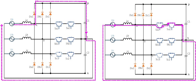
Fig. 2 Flow path with positive three-level Vienna current
0 level: When the switch Sa1 is turned on, the A-phase output is zero level, that is, UAN=0. The current flow path is: flowing out from the positive pole of the A-phase power grid, passing through the inductor La, then flowing through the reverse diode of the switch tube Sa1 and the switch tube Sa2 to the DC side midpoint N, and finally returning to the A-phase power grid through the other two phases. The specific flow path is shown in Figure 2(b). At this stage, the inductor La is charged to store energy, and the DC output capacitor supplies power to the later load.
When a phase current is negative:
-1 level: When the switch Sa2 is turned off, the output of phase A is negative, that is, UAN=-Udc /2. The current flows through the freewheeling diode Da2 and the inductor La, and finally flows into the power grid Ea. The specific flow path is shown in Figure 3(a). At this stage, the inductor La and the power grid Ea charge the capacitor and supply power to the post-load.
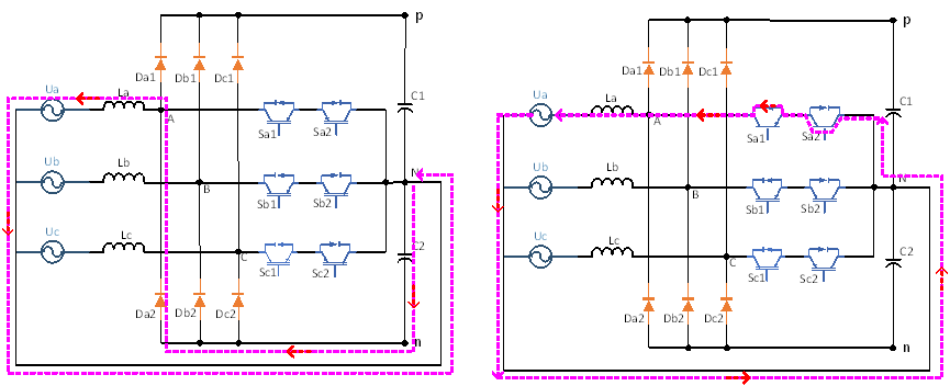
Fig. 3 Flow path with positive three-level Vienna current
0 level: When the switch Sa2 is turned on, the A-phase output is zero level, that is, UAN=0. The current flows through the reverse diode of the switching tube Sa2 and the switching tube Sa1, and the inductor La, and finally flows into the power grid Ea. The specific flow path is shown in Figure 3(b). At this stage, the inductor La is charged reversely to store energy, and the capacitor supplies power to the later load.
Loss analysis of IGBT
IGBT module is mainly composed of IGBT and FRD, which will produce two parts of loss correspondingly. As shown in Figure 4, IGBT loss mainly includes switching loss and on-state loss, while FRD mainly includes reverse recovery loss and on-state loss. On-state loss is caused by current flowing forward through IGBT or FRD, resulting in a certain voltage drop. Loss is the product of forward current and forward voltage drop across the device, and switching loss and reverse recovery loss are related to DC voltage and switching current during switching. For IGBT and FRD, the main factors affecting their on-state losses are: on-state current, junction temperature and switching duty ratio; The main factors that affect the switching loss are collector current, junction temperature, driving resistance, parasitic capacitance and the voltage that the switching frequency device bears when it is turned off.
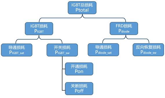
Fig. 4 IGBT loss composition
Taking the three-phase Vienna of 30kW charging pile module as an example, the IGBT and FRD losses are calculated respectively.
Total IGBT loss:
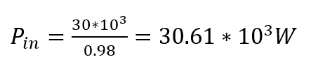
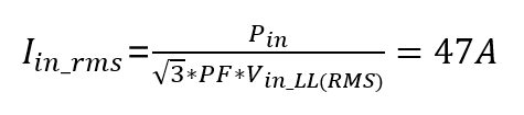
For the unidirectional charging pile module, it is usually composed of three-phase Vienna PFC in the front stage and LLC topology in the back stage. Assume that the three-phase Vienna input line voltage of the charging pile module is 380V, the output DC voltage is 800V, the PFC efficiency is 98%, and the power factor PF value is 0.99.
Then the input power
Effective value of input phase current
 Input line voltage
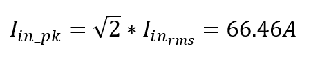
Input phase current peak value
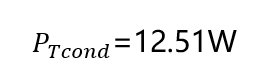
Because a single IGBT is only responsible for the positive half-cycle (or negative half-cycle) current flowing, the on-state loss of a single IGBT is:
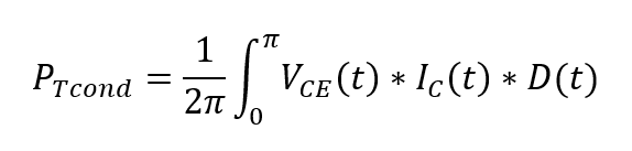
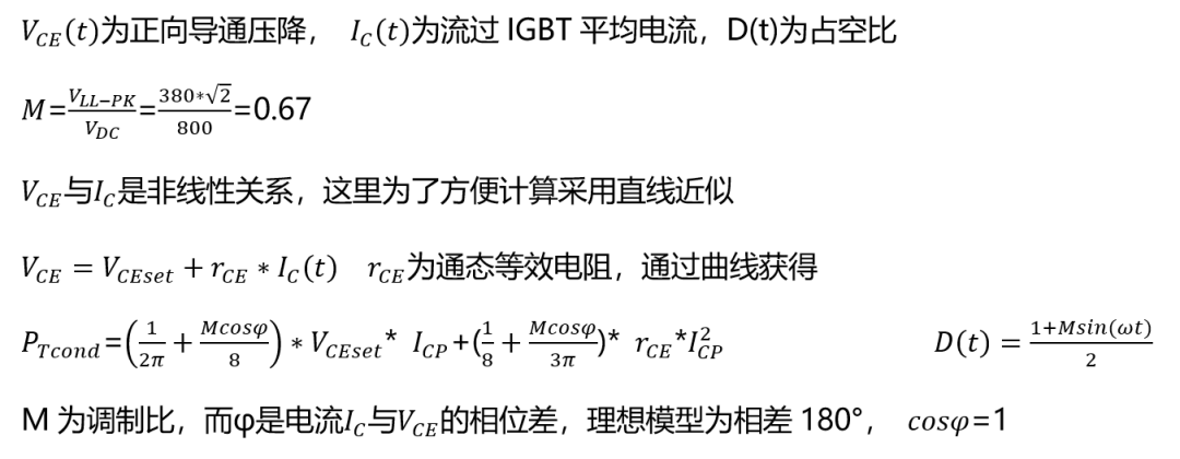
Because 30KW usually adopts two parallel devices and two series devices, when the temperature is 125 and Ic=30A according to the specifications of Alkaidsemi AKB65A50WHS,

=1.549V , Eon=0.646mJ,Eoff=0.2mJ。
The switching frequency is calculated at 27kHz.
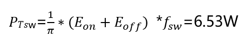
The total loss of 12 IGBT is ptotal = 12 * (12.51+6.53) = 228.48 w.
FRD loss:
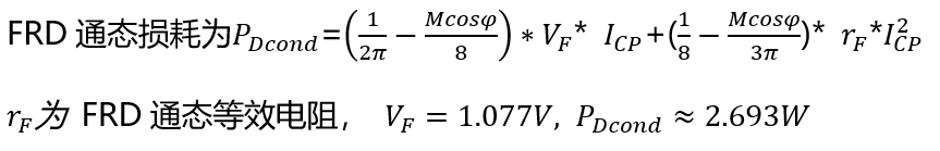
The reverse recovery loss of FRD is relatively small, so it is ignored here.
The total loss of 12 FRDs is p Diode = 12 * 2.693 = 32.32 W.
Summary: In the 30kW charging pile, the main loss source of IGBT is conduction loss, and the total loss is mainly determined by Vcesat at high temperature.