Foreword
The avalanche of MOSFET mainly involves that under certain conditions (such as high voltage or high current), more electron-hole pairs are generated inside it through collision ionization, which leads to a sharp increase in current and affects the performance of the device. Avalanche characteristic is an important parameter to be considered in the design and application of MOSFET, because it is directly related to the safe operation and reliability of the device.
Avalanche definition
MOSFET avalanche refers to the phenomenon that when the voltage on MOSFET exceeds its breakdown voltage, under the action of strong electric field, carriers (electrons and holes) gain high enough energy to produce new electron-hole pairs through collision ionization, forming a chain reaction, resulting in a sharp increase in current. This phenomenon is similar to an avalanche. The initial small amount of carriers in the strong electric field quickly leads to the generation and flow of a large number of carriers, which may cause damage to MOSFET devices and affect their normal operation and performance.
Avalanche current and avalanche energy
The avalanche characteristics of MOSFET include avalanche current (IAS and IAR) and avalanche energy (EAS and EAR). Among them, EAS represents the single avalanche breakdown energy, that is, the reverse avalanche breakdown energy that the device can safely absorb; EAR stands for repetitive avalanche energy, which calibrates the repetitive avalanche breakdown energy that the device can withstand. The limiting condition of these parameters is usually the maximum allowable junction temperature of the device (TCH < = 150℃).
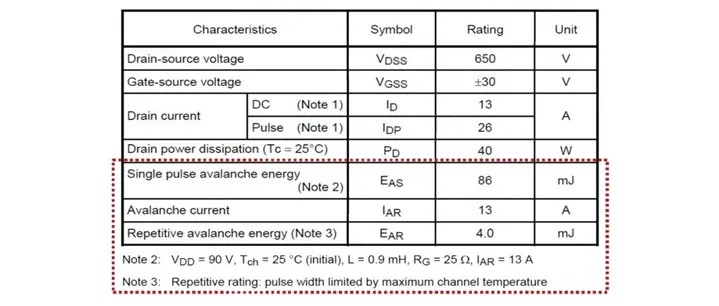
Figure 1 avalanche capability of MOSFET
Avalanche failure mechanism
As shown in the basic principle circuit diagram and test waveform in Figure 2, when MOSFET is used in inductive load applications (such as inductors, transformers, motors, etc.), when MOSFET is turned off, due to the characteristics of inductance or circuit parasitic inductance, back electromotive force is generated, and this back electromotive force will be superimposed on the input voltage to generate a high voltage exceeding the maximum rated value (VDSS) of MOSFET.
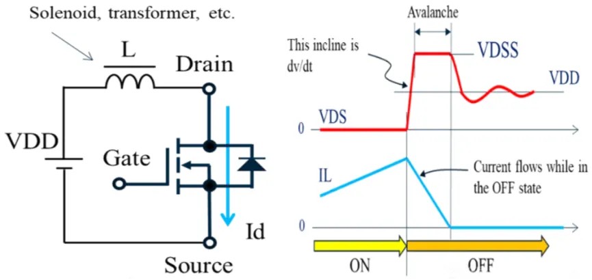
Fig. 2 Basic principle circuit diagram and test waveform
Breakdown occurs when a voltage higher than the absolute maximum rating BVDSS is applied to the MOSFET. When a high electric field higher than BVDSS is applied, the free electrons are accelerated with great energy, which will lead to collision ionization, thus producing electron-hole pairs. This phenomenon of avalanche increase of electron-hole pairs is called "avalanche breakdown". During this avalanche breakdown, the current flowing in the opposite direction to the diode current inside the MOSFET is called "avalanche current IAS", as shown in the blue path in Figure 3.
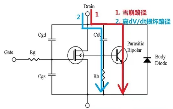
Fig. 3 avalanche mechanism of MOSFET
During avalanche breakdown, not only the short circuit and damage caused by the misleading conduction of parasitic triode caused by avalanche current (as mentioned above), but also the damage caused by excessive heat caused by conduction loss will occur. When MOSFET is in breakdown state, avalanche current will flow. According to the waveform shown in Figure 1, the avalanche energy formula in this state is
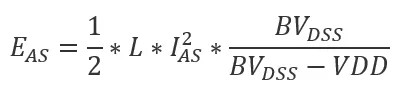
This power loss is called "avalanche energy EAS". Although MOSFET is OFF, the current will still flow from tens of amps to hundreds of amps. On the one hand, it will produce high loss and high temperature, which may damage the cell structure of MOSFET. On the other hand, excessive avalanche current will lead to the conduction of parasitic triode of MOSFET, which will make the drain-source of MOSFET tend to be on at high voltage, and the drain-source current will increase greatly in an instant, resulting in the failure of MOSFET.
Application conditions and preventive measures of avalanche
In practical application, avalanche damage often occurs under extreme conditions such as overvoltage, overcurrent and high temperature. For example, at high temperature, system output short circuit and overload test, input overvoltage test, dynamic aging test, etc., the damage of MOSFET should be considered first.
-
Accelerate the system response of short circuit to reduce the drain current during turn-off;
-
Optimize circuit and transformer design to reduce leakage inductance and line stray inductance;
-
Add buffer circuit to suppress di/dt.
In the application of flyback converter, due to the leakage inductance of transformer, a large voltage spike will occur when MOSFET is turned off, which is mainly composed of input voltage+output reflected voltage+leakage inductance induced voltage. At this time, avalanche energy should be considered, and some protective measures (such as strengthening RCD clamp circuit and RC absorption circuit, etc.) should be added when necessary to ensure that MOSFET is not damaged.
In the motor drive circuit, because the windings of some motors are inductors, for the inductive load, the motor will generate a great impact current during starting and blocking, which also produces a great current change when the MOSFET is turned off, resulting in the avalanche breakdown of the MOSFET.
To sum up, in order to protect MOSFET from avalanche breakdown, relevant protection measures can be taken for different applications, such as connecting RCD absorption loops at both ends of transformer (inductive load) in parallel to reduce reverse peak voltage; The gate resistance is connected in series and set to an appropriate value to suppress dv/dt and increase the turn-off time to suppress the reverse spike voltage; Connect RC absorption loop in parallel between DSs of MOSFET to absorb reverse spike voltage; The wiring of high current circuit is thickened and the distance is shortened to reduce parasitic inductance.
Summary
The avalanche characteristic of MOSFET is an important physical phenomenon under the condition of high voltage or high current, which has a direct impact on the safe operation and reliability of the device. These characteristics should be fully considered in design and application, and appropriate protective measures should be taken to ensure the reliable operation of MOSFET.