Foreword
Compared with Si devices, the third generation wide band gap semiconductor material SiC has the advantages of faster switching speed, higher withstand voltage and better temperature characteristics, which correspondingly brings less loss, smaller volume of magnetic components in the system and higher power density. However, with the continuous increase of switching frequency of SiC MOSFET, the crosstalk of bridge arm in half-bridge structure (such as inverter circuit, full-bridge circuit, etc.) becomes more and more serious, which is easy to cause direct short circuit of bridge arm or affect reliability, which limits the further improvement of switching frequency and system power density of SiC MOSFET.
Causes of crosstalk
-
Switching speed: SiC MOSFET has faster switching speed, and produces high dv/dt (voltage change rate) and high di/dt (current change rate) at the moment of switching action.
- Barotropy dv/dt:在The displacement current flowing to the driving side is generated on the Miller capacitor (Crss, the capacitor between the drain and the gate in MOSFET), which causes a forward induced voltage on the gate impedance, and the superposition on the gate source will cause the gate source voltage to rise.,
- Subatmospheric pressure dv/dt :A displacement current flowing to the device side is generated on the Miller capacitor, and a negative induced voltage is caused at the gate impedance, resulting in an excessive negative voltage peak at the gate source.
-
Circuit parasitic parameters: In circuit structures such as half-bridge topology, there are parasitic inductances and capacitances in the lines, which interact with devices to produce crosstalk when the switch is operated.
-
Analysis of crosstalk process with half-bridge circuit as an example;
- Forward crosstalk:
When the gate voltage of the upper tube reaches the threshold, the channel is opened and the current is reversed. At this time, the diode of the lower tube bears the reverse voltage, and the voltage of Vds2 rises rapidly. The Miller effect produces a displacement current and a voltage drop at its gate. Lg is the gate lead inductance. After the displacement current Ig flows through Lg2, it can be known from Lenz's law that the induced electromotive force VLg2 is left negative and right positive, and Vgs2=-V2+(VLg2+VRg2).
In the formula, -V2 is the negative voltage driven by SiC, VLg2 is the induced voltage of parasitic inductance, and VRg2 is the voltage generated by internal Rg. Therefore, when the upper tube is turned on, the crosstalk voltage of the lower tube Vgs is VLg2+VRg2. If this voltage exceeds the turn-on threshold voltage Vth, it will lead to the possibility of up-and-down direct connection.
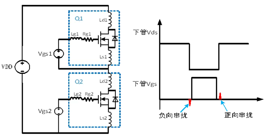
Fig. 1 Opening and crosstalk process of upper and lower tubes
- Negative crosstalk:
When the gate voltage of the main upper tube reaches Miller voltage, its drain-source voltage begins to rise and the lower drain-source voltage Vds2 begins to fall, as shown in Figure 1. At this time, the crosstalk voltage generated at the gate of the lower tube is the same as the forward crosstalk formula, but the change rate of voltage and current is different, and the negative voltage may exceed the rated gate negative pressure, which will affect the reliability of the gate.
Crosstalk effect
-
May cause short circuit of bridge arm: If the forward crosstalk voltage makes another switch tube that should have been turned off partially or completely turn on, it will cause the upper and lower bridge arms to turn on at the same time, forming a short circuit path.
-
Grid damage: If the negative crosstalk voltage exceeds the negative rated voltage of the gate of SiC MOSFET, it will cause the gate to be overstressed, which may lead to the damage of the gate for a long time.
-
Limit switch speed: The crosstalk problem in the operation of SiC MOSFET may limit the original SiC MOSFET to achieve higher switching speed.
Suppression measures
-
Reduce the switching speed: It is the most intuitive, but it limits its high-frequency advantage and makes the system efficiency and power density somewhat discounted.
-
Select the appropriate negative driving voltage: Choose a compromise so that the positive crosstalk is not higher than the threshold voltage and the negative crosstalk is not higher than the rated negative voltage (although it is difficult to choose, it often needs many experiments based on the existing system).
-
Add auxiliary circuit: Adding auxiliary circuits (such as MOSFET, BJT, etc.) to the gate circuit provides a low impedance path for crosstalk, but it increases the difficulty and cost of driving design.
-
Optimizing design to reduce parasitic parameters: When designing, the parasitic inductance and capacitance should be as small as possible.
-
Technical improvement
- Reduce the impedance of the gate lead: thereby reducing the induced voltage drop on the impedance and suppressing the overvoltage of the gate and source.
- Active miller clamping technology is adopted: the displacement current is released to effectively protect SiC MOSFET devices.
- Through the three-stage turn-off crosstalk suppression technology, the gate driving waveform is improved, and the excessive positive voltage rise and negative voltage are effectively suppressed. -
Device selection: Choosing a silicon carbide device with low Miller capacitance (Crss) can improve the anti-interference ability of the device and reduce the risk of misleading the device under crosstalk.