Foreword
LLC resonant converter power device is one of the isolation topologies that has attracted much attention in recent years because it can realize ZVC and ZCS, and has high efficiency, small size and high power density. In the application of low voltage and high current output, synchronous rectification, SR) technology is adopted at the secondary output side to reduce the power loss of diode rectification, which can greatly improve the heavy and full load efficiency.
LLC synchronous rectification control method
The key of LLC synchronous rectification technology is to control the driving signal of SR MOSFET. At present, the mainstream schemes in the market are basically controlled by detecting the drain-source voltage of SR MOSFET. Common synchronous rectification control IC are IFX-IR11682S, IR11688, ON-NCP430X series, NXP-TEA 1995 and Ti-UCC24610. Figure 1 shows the typical application of synchronous rectification IC NCP430X series in LLC synchronous rectification and its related waveforms.
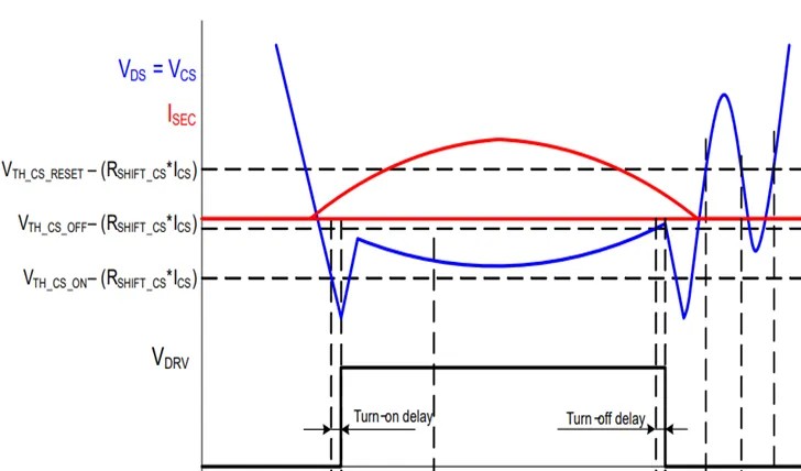
Fig. 1 schematic diagram of NCP 430x series control scheme
Before the SR MOSFET is turned on, the current flows through its body diode. The direct voltage drop of the body diode is usually 0.6-1V, and the control chip detects this voltage and triggers Vth_on. In order to avoid the spike false trigger caused by resonance, it is necessary to turn on the driving signal after a Turn-on delay time.
After the MOSFET is turned on, the current flowing through its channel is sinusoidal. When the current gradually decreases, the VDS voltage also approaches zero, which triggers Vth_off. After the same Turn-off delay time, the driving signal is turned off, and the current goes to the body diode, and the VDS voltage jumps negatively again, and finally the zero current is turned off.
Efficiency optimization of LLC synchronous rectification
In the application of PC power supply and server power supply, the output current is tens of amperes or even hundreds of amperes. In order to obtain higher system efficiency, several MOSFETs with smaller Rds_on are usually selected in parallel. At present, our company adopts shielded gate trench MOSFET (SGT MOSFET), and the Rds_on has been reduced to 0.5mΩ (withstand voltage 40V). Under certain RDS _ ON conditions, the efficiency can still be improved by optimizing the peripheral driving parameters and Layout. Its core idea is to increase the conduction time of MOSFET channel and reduce the conduction time of body diode.
In practical application, it often happens that the driving signal is turned off long before the sine wave reaches zero. As shown in fig. 2, in fig. 2, the Drain Current (green) is the current waveform flowing through the MOSFET channel, and the DRV (blue) is the SR-MOSFET VGS driving waveform. After the MOSFET channel is turned off, the body diode freewheels, and the voltage drop of the body diode brings great conduction loss. In this application, the driving signal DRV (blue) should wait until the sine wave current is close to zero, so as to make full use of the advantages of synchronous rectification.
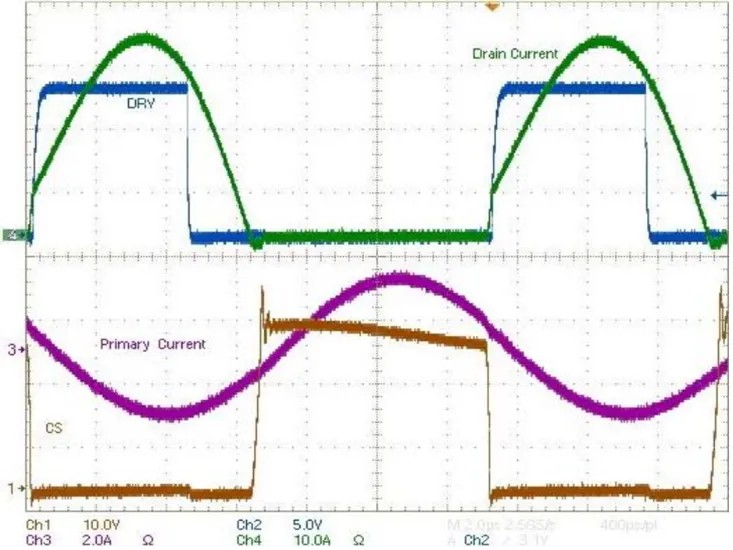
Fig. 2 waveform diagram of MOSFET channel early turn-off in practical application
This phenomenon is mainly caused by the wiring inductance or packaging parasitic inductance Lpackage of MOSFET, as shown in Figure 3. Where L_drain is the lead inductance of the drain, L_source is the lead inductance of the source, and Rds_on is the on resistance. In fact, the synchronous rectification control IC VDS detects voltage besides Rds_on, as well as MOSFET parasitic inductance and PCB wiring inductance (tens of nH). Because the inductance hinders the current change, the current IDS at both ends of the detection network lags behind the voltage VDS (the voltage VDS leads the current IDS). When the VDS voltage triggers the turn-off threshold (close to zero), it turns off early after the Turn-off delay time, but in fact, IDS has not dropped to zero when VDS crosses zero.
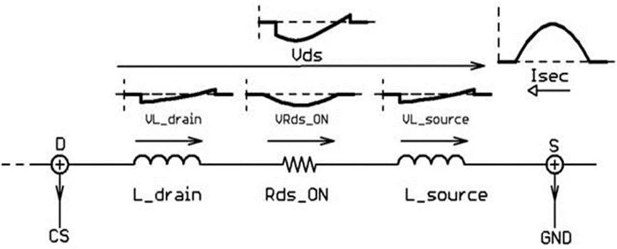
Fig. 3 schematic diagram of MOSFET channel early turn-off in practical application
Optimization idea 1: Increase the RC filtering of VDS detection circuit and delay the detected advanced voltage for a period of time. The delay can be satisfied if the relation R*C=Rds_on/Lwire(Lwire package inductance+package wire inductance) is satisfied. The disadvantage of this scheme is that the opening may also be delayed.
Optimization idea 2: The VDS detection loop uses Kelvin connection to reduce the parasitic inductance of PCB (try to use patch devices, and the packaging wiring inductance is smaller than TO-247).
Optimization idea 3: Choose MOSFET with lower Vth value (turn on early and turn off late, increase the channel on time of MOSFET and reduce the body diode on time).
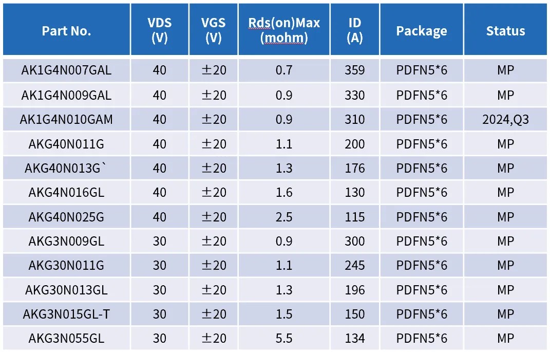
Product selection of Alkaidsemi SGT SR scheme