Foreword
Because MOSFET is a voltage-type device, it can be turned on when the driving voltage Vgs is greater than the voltage Vth. Turning on is the process of charging the parasitic capacitor, and similarly, turning off is the process of discharging the parasitic capacitor.
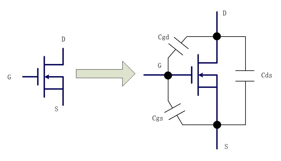
Stray capacitance
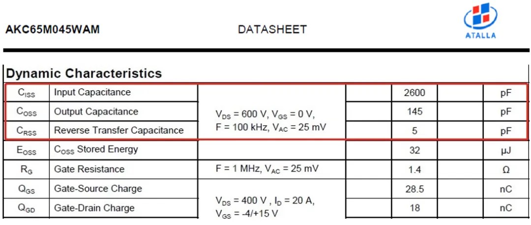
Input capacitance Ciss=Cgs+Cgd, measured by DS short circuit.
Output capacitance Coss=Cgd+Cds, GS short circuit, Cgd and Cds in parallel.
Reverse transmission capacitance Crss=Cgd, also called Miller capacitance. This capacitance is not constant, it changes rapidly with the change of voltage between G electrode and D electrode, and it will also affect the charging of G electrode and S electrode capacitance.
Opening process
Vth——The turn-on threshold voltage between the GS electrodes of a MOSFET, which is completely labeled as VGS(th), is one of the important parameters of the MOSFET, and is generally simply labeled as Vth, and is defined as the minimum gate bias that can form a conductive channel between the source and the drain.
VP——Miller step voltage refers to the voltage value at which the gate voltage remains stable for a certain period of time during the switching process of MOSFET. During this time period, the gate voltage does not change with the change of gate current.
-
0-t1 (cut-off area): In the stage before the arrival of VGS, when the MOSFET is not turned on at all, the circuit is essentially an RC charging and discharging circuit. As shown in the following figure, the Id of this stage is equal to 0, and the MOSFET is in the off state.
-
T1-t2 (saturation zone): The MOSFET starts to "loosen", and the Id starts to increase from 0, which increases linearly according to the form of a voltage-controlled current source and a certain slope. The slope is determined by the transconductance of this voltage-controlled current source. At this stage, the drain current of MOSFET begins to flow, and VDS still keeps Vdd. This rising ramp continues until the end of the second stage, when the current Id reaches saturation or the maximum load current, and VGS rises to the Miller platform voltage VP.
-
T2-t3 (Miller District): VGS is limited to a fixed value (the transmission characteristic of MOSFET), so during this period, Cgs no longer consumes charge, and the driving current instead flows to Cgd to charge it (Cgd discharges first and then charges, and the polarities at both ends are reversed). As VDS decreases from high voltage to Id*RDS(on), Cgd also increases with VDS decreasing, so the charge required for Ig to charge Cgd is relatively large. Therefore, the size of Cgd capacitor directly affects the switching time of MOSFET. For fast switching applications, try to reduce the platform time.
-
T3-t4 (linear region): With the continued charging of Ig, VGS entered the linear rising stage again. At this time, the drain voltage drops to VDS =Id *RDS(on), and at this time, the working state of MOSFET enters the resistance region, and the gate voltage is no longer affected by the drain current to rise freely.
Turning off MOSFET is the reverse process of turning on MOSFET.
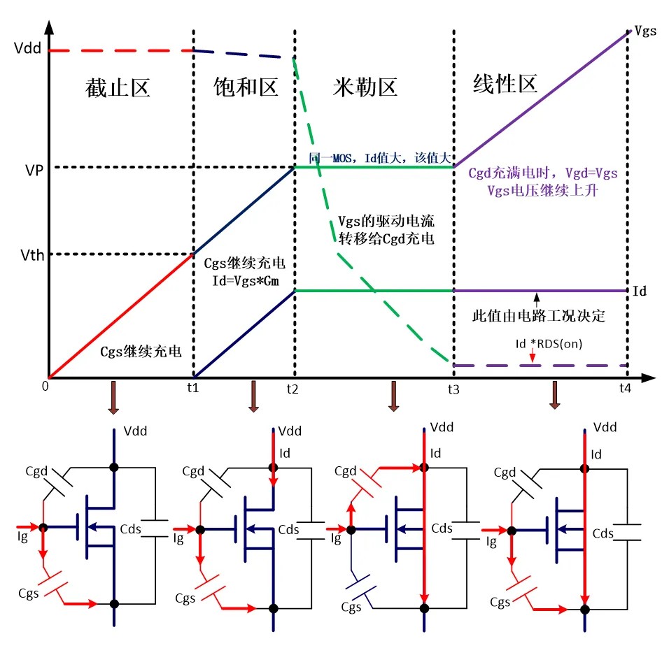
Focus on discussion: In Miller area, when the D-pole voltage starts to change, a very large dv/dt will be generated. Through the capacitor Cgd, the generated current is:
This current is large enough to draw all the current that can be provided by the driving circuit. Almost all the current of the driving circuit flows through Cgd to remove the charge stored in the Cgd capacitor (Miller capacitor), so that almost no current flows through the Cgs capacitor, and the gate voltage remains basically unchanged. It can be seen that Vgs maintains a platform voltage for a period of time t2- t3. Miller platform voltage is determined by the maximum current Id(max) of the system and the Vth and transconductance of MOSFET.
With the continuous decrease of Vds voltage, the absolute value of Vgd voltage also decreases, and the voltage of Vgd changes from negative to zero, and then begins to increase positively. When the Vds voltage is reduced to the lowest value, the charge of Miller capacitor is basically completely swept away.